
MANUFACTURING IDEAS TO WATCH
CHEMICAL VAPOR DEPOSITION OF WATERPROOF COATINGS ON NATURAL FIBERS
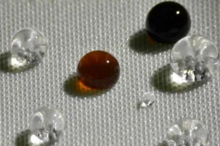
Researchers at the Massachusetts Institute of Technology used a recent variation of chemical vapor deposition (known as initiated CVD, or iCVD) to deposit short chains of perfluorinated polymers on cotton, nylon, linen, and even paper. Long-chain perfluorinated polymers, typically deposited on fabrics using solvents, are undesirable as they persist in the environment. Since CVD is a gaseous method, it coats all fibers individually and uniformly down to the micrometer level with less waste, and therefore a smaller impact on the environment. The method also offers longer lasting water-proof coatings as solvent-based approaches typically only coat the outside of the fiber bundles
– Kripa Varanasi, Massachusetts Institute of Technology
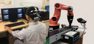
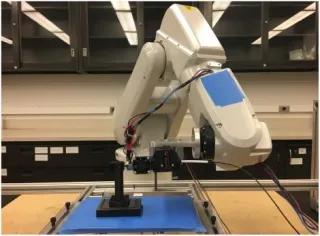
MIND-READING QUALITY CONTROL
Engineers at the University of Illinois Urbana-Champaign designed a quality control robotic system that uses brain-computer interface to remove parts from an inspection line based on human thought. A human is shown images of the parts in the production stream. An assembly-line robot can read the electrical signals from a person’s brain to detect when he or she has spotted a defective part. Such a system could have broad repercussions, such as remote staffing of quality control staff, job opportunities for disabled personnel, and accelerated quality control.
– Yao Li, University of Illinois Urbana-Champaign
SELF-HEALING POLYMERS MOVING FORWARD
A team lead by researchers at Oak Ridge National Laboratory developed a self-healing polymer that can be stretched a whopping 5,000%. To demonstrate its self-healing properties, they made a gas separation membrane with the polymer and tore it. Left to self-repair for 2 hours at room temperature, the membrane restores its mechanical properties and even separated the gases as well as before it was torn. The polymer is a urea-functionalized silicone (polydimethyl siloxane). The self-healing properties of the material can extend the lifetime and reliability of manufactured components.
– Tomonori Saito, Oak Ridge National Laboratory
TITANIUM AND CARBON FIBER ULTRASONIC BONDING
Stacks of carbon fiber reinforced polymer (CFRP) and titanium are used in load-bearing components of large commercial aircraft because they combine the wear resistance and elastic modulus of titanium with the strength-to-weight performance of CFRP. The current methods for joining CFRP/titanium stacks, whose application can account for up to half the cost of manufacturing the part, are rivets and bolts (which cause stress concentrations), or adhesives (which are not as strong). Alternatively, ultrasonic bonding “shakes” materials together, interlocking them, for uniform, strong, and low temperature bonding. Researchers from California State University, Fullerton have successfully extended ultrasonic bonding to CFRP and titanium.
– Sagil James, California State University, Fullerton
TURNING FOOD PROCESSING WASTE INTO USEFUL BIOGAS
Food manufacturing and processing often produces fats, oils, and grease (collectively known as FOG waste) that can clog sewer lines if not processed appropriately for disposal. Biogas production is a common approach to processing organic waste, but is limited to inputs of 30% FOG due to harm it causes to the bacteria in the bioreactor. A team of engineers at University of British Columbia developed a method to process FOG that converts up to 80% of it to fatty acids that biogas digesters can tolerate. The process, known as microwave-enhanced advanced oxidation, uses microwaves and hydrogen peroxide to breakdown long-chain fatty acids into short-chain known to increase biogas production. This technology should benefit food manufacturers, municipal water treatment plants, and even farmers, by turning a waste liability into an energy-recovery opportunity.
– Kwang Victor Lo, University of British Columbia

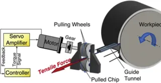
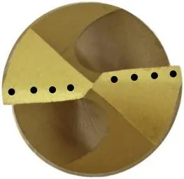
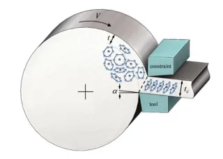
CHIP-PULLING FOR REDUCED CUTTING ENERGY AND TOOL FORCE
Researchers at Oregon State University have developed a novel turning system that reduces cutting energy, improving both tool life and turning performance. The system uses an external pulling device that guides and actively pulls chips away from the cutting surface. The system monitors the chip-pulling tension for real-time cutting control. Such control can allow for zero thrust force during cutting, where no normal force is needed between the cutting head and the part. This is critical for turning slender parts without causing errors from part deformation.
– Burak Sencer, Oregon State University
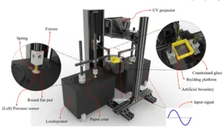
IMPROVING STEREOLITHOGRAPHY SEPARATION USING VIBRATIONS
Stereolithography has emerged as the preeminent additive manufacturing processes for high precession parts, however, the process faces challenges in repeatedly separating the build layer from the constraining surface. While others, such as Carbon 3D, have addressed this using an oxygen permeable membrane, these solutions do not typically scale well to larger sizes. Researchers at University of Southern California have developed a novel system for reducing this separation force with vibrations. By sending an acoustic signal to the constrained glass surface, the separation force can be reduced by up to a factor of 3. This very low-cost solution has the potential to improve both build quality and build area.
– Yong Chen, University of Southern California
TOWARDS LOW-COST DIAMOND ELECTRONICS
Diamond is the ultimate material. But producing diamond films good enough to make microelectronics, spintronics, power electronics, hardened radiation electronics, and a host of other critical and strategic applications, is estimated to cost upwards of $10,000 per wafer. A more affordable method, known as High Pressure High Temperature, traditionally results in widespread dislocation defects and more impurities. Researchers have found that applying the right growth geometry (the inclined plane of a pyramidal shape substrate) combined with optimized growth conditions with Plasma Assisted Chemical Vapor Deposition (PACVD) technique allows the dislocations to be greatly decreased. It also allows for the defects to be confined and defect-free regions to be produced. While this approach still has a ways to go before mass production, the approach is underpinned by phenomena exploited in the growth of Ge/Si films, providing promising prospects for reasonably-priced, manufacturing-grade, diamond substrates.
– Amine Boussadi & Jocelyn Achard, Process and Materials Sciences Laboratory, University of Paris 13
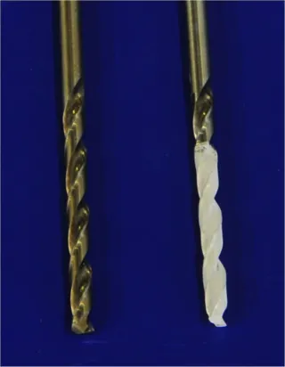
REAL-TIME DRILL BIT HEALTH MONITORING
Drilling is one-third of all machining operations and tends to happen later in the manufacturing process; therefore, it is important to get it right. This can be challenging when drilling superalloys because the material makes drill bits wear and break prematurely at random. Georgia Tech Researchers and collaborators are working to develop reliable and inexpensive ways to predict bit wear. They put neural networks to task by feeding them data from the spindle while drilling superalloy Inconel 625. The best performing algorithm (Conjugate Gradient Descent) predicted most instances of wear to within 8% with only 5 “neurons”, few enough that can be implemented in an embedded processor. They also found that while spindle force data, a parameter often used in this kind of study, results in a more accurate prediction than spindle power consumption, spindle power (which is easy to measure and most industrial presses have a built-in sensor for) did a decent job, too. This work paves the way for compact, inexpensive, non-invasive retrofit systems to usher smart manufacturing into the factory floor.
– Thomas Kurfess, Georgia Tech
“WRITING” GRAPHENE ON ORGANIC MATERIALS
Researchers at Rice University are transforming carbon-based materials into graphene by perfecting laser-induced graphene (LIG) production, a process for which lignin, a non-edible carbohydrate present in most plant-based materials, serves as a good graphene precursor. They have successfully made graphene patterns and even electrical circuits on the surface of paper, cork, a potato, and even toast. In the LIG process, a first pass of a laser slightly “burns” the material, turning the surface into amorphous carbon. Then, a second laser with precisely controlled parameters converts the burn marks into graphene of enough quality to make electrical circuits (sheet resistance of 15 Ohm/sq. that allowed to demonstrate a capacitor made thusly). The process works in regular atmospheric conditions, uses an inexpensive CO2 laser, and is fast enough to be integrated into existing production lines. Writing RFID tags directly on cardboard boxes for logistics and inventory control is specifically attractive application.
– James Tour, Rice University

SIX-AXIS ADDITIVE-SUBTRACTIVE MANUFACTURING
Additive manufacturing provides the opportunity to create complex geometries with minimal material waste, yet it is often held back by relatively poor surface quality, dimensional accuracy, “staircase” errors, and production time. Researchers at University of Illinois, Chicago have developed a novel 6-axis hybrid additive-subtractive manufacturing process. While hybrid additive-subtractive processes have been explored, this process utilizes 6-axis motion to leverage the advantage of the additive and subtractive aspects of the process. For example, dynamic adjustment of the object and tool axis can eliminate the need for support structures and create high quality freeform surfaces. This process has the potential to improve surface quality, dimensional tolerances, and production speed.
– Lin Li, University of Illinois at Chicago
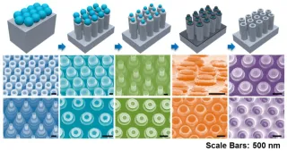
SCALABLE THREE-DIMENSIONAL NANOSTRUCTURE FABRICATION
Three-Dimensional nanostructures have a wide variety of applications, including biosensors, drug delivery, electronic sensors, optics, and solar cells. While many of these structures can be produced using electron-beam lithography, the process is complex, costly, and has low throughput. Researchers at UCLA have developed a fabrication method that enables high-throughput lithography. Nanosphere lithography uses an array of nanospheres as resists. By etching the nanospheres at each step to create the desired resist pattern for the subsequent step, the process can generate complex three-dimensional patterns. It enables the scalable production of hierarchical nanostructures with tunable diameters, heights, and pitches, including the multi-level nanotowers generated in this study.
– Paul Weiss, UCLA
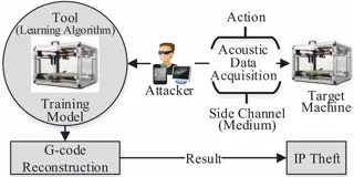
INTELLECTUAL PROPERTY THEFT USING ACOUSTICS OF ADDITIVE MANUFACTURING
Additive manufacturing is increasingly being used to produce parts that involve sensitive intellectual property (IP). Accelerating implementation and innovation in additive manufacturing relies on understanding how this valuable IP is vulnerable and devising systems to protect it. Researchers at University of California, Irvine discovered that acoustics can be used to perform a side channel attack. In this attack, acoustic information is gathered from the additive manufacturing system, captured from the sounds created by the stepper motors that drive the internal components. The G-code, containing information about the movement and speed of the deposition head, can then be reconstructed from this acoustic information. Finally, the G-code can be used to reconstruct the underlying design and steal the intellectual property. This has been demonstrated on fuse deposition manufacturing systems, demonstrating the critical need to discover and implement protections for additive manufacturing systems.
– Mohammad Al Faruque, University of California, Irvine
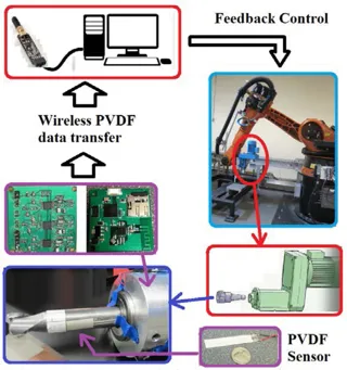
WIRELESS FORCE SENSORS IMPROVE ROBOTIC MILLING ACCURACY
Robotic milling machines reduce capital investment costs and equipment footprints while improving flexibility and versatility, as compared to traditional multi-axis machining centers. However, robotic milling can only provide limited accuracy. Researchers at Georgia Tech demonstrated that in situ wireless force sensors can be used to measure milling forces in real-time, providing opportunities for real-time tool position correction and ultimately improving accuracy. Using a model of the mechanics of the robotic milling machine, a closed-loop controller provides corrective feedback to the robot’s controller, allowing for greater than 70% improvement in the dimensional accuracy. This technology holds promise for large area, low-cost, multi-axis machining.
– Shreyes N. Melkote, Georgia Tech
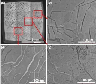
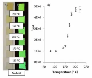
THERMOCHROMIC POLYMERS FOR EARLY DETECTION OF THERMAL DAMAGE IN COMPOSITES
Early detection of damage to carbon fiber-epoxy composites is crucial for ensuring safety in critical applications, such as aerospace components. Thermal damage detection is especially difficult as it presents as chemical, rather than mechanical degradation. Existing ultrasonic non-destructive testing methods are not able to detect this damage until it has progressed to later-stage cracks and delamination. Researchers have developed a thermochromic polymer that changes both color and fluorescent intensity when exposed to specified temperature-time combinations. These time-temperature combinations can be tuned to match the conditions that cause damage to composites. When applied as either a large area sheet or as a small sensor, this material provides easy visual detection of early-stage thermal damage. This technology has applications in vehicles, passenger aircraft, and renewable energy sectors as they transition to ubiquitous use of composites.
– Ryan Toivola, University of Washington
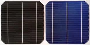
NEW SOLAR CELL MATERIAL FOR MASS ADOPTION
Silicon-based solar cells max out in efficiency at about 20%. Higher efficiency requires silicon alternatives, but the best performing ones tend to be rare or toxic, limiting massive, large scale adoption. For example, gallium arsenide can provide an efficiency of 46%, but gallium is rarer than gold and arsenic is toxic. Prof. Pierre Ferdinand Poudeu of the University of Michigan Material Science and Engineering Department, has been investigating alternative solar cell materials that provide high efficiencies while also being safe, abundant, and inexpensive. His team discovered a promising candidate made of copper, titanium, and selenium (Cu4TiSe4). In addition to being nontoxic and from abundant elements, the fabrication process, based on powder and pulse laser deposition, uses less materials and is cheaper than molecular beam epitaxy used for GaAs films. The absorption coefficient of the new material in wavelengths of peak solar irradiation are 5 to 10 times greater than established high-efficiency photovoltaic materials, suggesting that one day it could exceed current efficiency records.
– Pierre Ferdinand P. Poudeu, University of Michigan

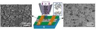
CONTINUOUS MANUFACTURING OF HIGH QUALITY GRAPHENE
Researchers at MIT have developed and demonstrated a continuous manufacturing process for producing high-quality graphene. This scalable production method produces graphene membrane filters, with applications including biological separation, desalination, and gas permeable barriers, and more. The process employs a scalable, roll-to-roll approach, depositing the graphene on thin foils using a two-zone chemical vapor deposition system. The graphene is then taken up by a second spool, where it is post-processed to create functional devices. Controlling the temperatures and feed rates of the process enables precise control over the graphene properties, and the creation of seamless, endless sheets.
– John Hart, MIT
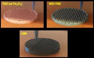
3D-PAINTING: MULTI-MATERIAL CERAMIC ADDITIVE MANUFACTURING
Additive Manufacturing of multi-material ceramics is essential for applications ranging from fuel cells to biomedical devices to defense. Researchers at Northwestern have developed a novel additive manufacturing process that uses 3D-paints to deposit the structure. This direct-write extrusion method uses specially designed paints that contain many of the same components as household paints, but use functional powders and particles, rather than pigments. Much like household paint, shear thinning polymers and a solvent mixture are added to enable deposition, with the solvent evaporating to leave the desired particles. These paints are also composed primarily of the functional particles, rather than the non-functional polymers, enabling final products with desired properties. The 3D-printed ceramic objects can be used as-is, or be thermally processed to burn away the polymer and to densify the ceramic as appropriate for the application.
– Ramille Shah, Northwestern University
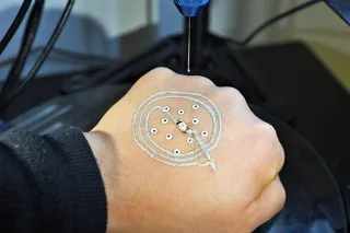
3D PRINTING ON IMPERFECT, MOVING SURFACES
Current additive manufacturing systems deposit material along a pre-programed path or pattern as an open-loop control system. Should anything go awry, like running out of material or accidentally bumping the part, open-loop systems have no way of compensating and as a result the build job is typically discarded. Alternatively, if you can detect and measure changes in real time, you enable high quality printing on non-uniform substrates like textiles or a living person in the case of skin. This is also widely applicable for automating the process of remanufacturing heavy machinery. Such a system requires a closed-loop feedback and control system. Researchers at the University of Minnesota have design such a system using computer vision to monitor a surface throughout the printing process and compensate the path of production in real time.
– Michael McAlpine, University of Minnesota
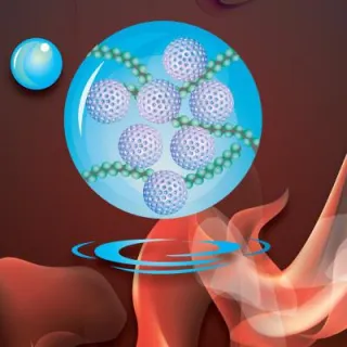
PLASTIC NEUTRON SCINTILLATOR CRYSTALS TO REPLACE EXPENSIVE, SCARCE MATERIALS
Neutron detection has broad applicability, ranging from cancer therapy and homeland security to non-destructive testing in manufacturing. But current neutron detection technologies sometimes struggle to distinguish between neutrons and gamma rays. Helium-3-based detectors are insensitive to gamma rays but world supplies of Helium-3 are in steady and imminent decline (since helium slowly sweeps out of the atmosphere and leaves the planet). Crystals of certain organic materials, like stilbene, make adequate detectors but are hard to grow and produce in large quantities. Liquid scintillators, another alternative, tend to be toxic. Polymer-based neutron scintillators have many advantages for large scale production, but their performance has lagged. A team of researchers at Lawrence Livermore National Laboratory has been improving plastic scintillators and recently reported that they are meeting or exceeding the performance of liquid scintillators. Their work may lead to a broader use of neutron detectors, especially in non-critical applications, like manufacturing, where cost is an important factor.
– Natalia P. Zaitseva, Lawrence Livermore National Laboratory
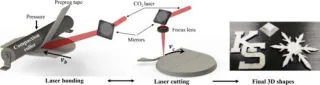
ADDITIVE MANUFACTURING OF HIGH-STRENGTH COMPOSITES
Researchers at Kansas State University have developed a method to additively manufacture composites with comparable strength to those made using traditional manufacturing methods, such as compression molding. The novel process uses a laser to bond and cut layers of fiber prepreg or tape to create 3D parts from continuous fiber reinforced thermoplastic composites. The resulting parts have 300% better strength than additive manufactured composites produced with fused deposition modeling. This process has applications in automotive, aerospace, marine, and other industries that will benefit from traditional composite properties with the versatility of additive manufacturing.
– Dong Lin, Kansas State University
CARBON NANOTUBE-BASED SENSING COMPOSITES
Structural health monitoring to measure the status of civil structures and buildings is critical to maintaining a robust infrastructure. Existing methods face challenges in obtaining real-time distributed measurements, especially at scales small enough to detect micro-cracks that lead to eventual failure. Researchers have developed a method to create a nanotube composite that couples axial strain of the material to a large change in electrical resistance. Electrical tunneling gaps between the carbon nanotubes increase as the material is strained. The carbon nanotubes are coated onto a carrier fabric to form the conductive network, and epoxy can then be added to form a stand-alone sensing “Smart Veil” with versatile applications. This “Smart Veil” can also be applied to polymer composites, enabling continuous feedback during processing.
– Erik T. Thostenson, University of Delaware and Thomas Schumacher, Portland State University
NOVEL NON-DESTRUCTIVE EVALUATION
Fatigue failure of aerospace parts can have disastrous results, as the recent accident of Southwest flight 1380 illustrates. Tools for identifying and studying fatigue cracking include acoustic emission, passive thermography, digital image correlation, and fiber optic sensors, but each of these methods has critical limitations. A team of researchers at NASA Langley Research Center developed a method that combines thermal and acoustic emission data to provide a much more sensitive evaluation tool than each alone. It can track multiple damage sites and identify false indications. The technique is applicable over large areas and for complex in-service parts.
– Joseph Zalameda, NASA Langley Research Center
WOOD STRONGER THAN TITANIUM
Researchers at the University of Maryland at College Park discovered a method to make natural wood 10x stronger by simply removing the lignin and hemicellulose, and pressing the resulting cellulose body. The resulting material has a specific strength (strength per unit mass) stronger than titanium. Ballistic testing also illustrates the resilience of the material to impact. The two-step process uses common chemicals and takes place at relatively low temperature. Using softwoods (like pine or balsa) gives similar properties as slower-growing wood, offering an additional environmental advantage.
– Liangbing Hu, University of Maryland
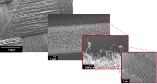
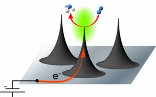
PHYSICAL CATALYSTS OFFER PATHWAY TO EFFICIENT AMMONIA PRODUCTION
Ammonia production is essential for fertilizer production, yet it accounts for 3% of the world’s energy use and contributes over 3% of greenhouse gas emissions worldwide. Researchers at Oak Ridge National Laboratory are developing a novel physical catalysts with promise to improve ammonia production. Unlike typical chemical catalysts, this physical catalyst uses spikes 50-80 nanometers high to amplify an electric field to a very strong 10 volts per nanometer. This enables the chemical reactions to take place without a chemical bond to the catalyst. Refining and scaling this method to industrial scale could provide a viable pathway to improved ammonia production.
– Adam Rondinone, Oak Ridge National Laboratory
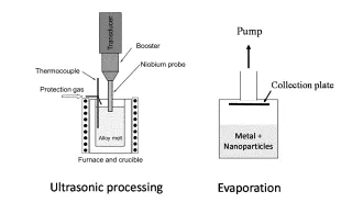
METAL MATRIX NANOCOMPOSITE PROCESS INNOVATIONS
Metal matrix nanocomposites (MMNCs) are lightweight, strong, and ductile materials with applications in a variety of industries including metal casting, defense, aerospace, automotive, and electronics. Their performance is enhanced by the ability to fabricate highly dense and uniform nanocomposites. However, current dispersion technologies struggle to uniformly disperse nanoparticles at the high densities necessary to yield high quality MMNCs. Researchers at UCLA developed a novel evaporation-based method to concentrate nanoparticles in an MMNC by partially evaporating the carrier metal from the carrier and matrix mixture. At the same time, a thermally activated self-stabilization mechanism ensures uniform particle distribution, resulting in the dense and uniform nanoparticle dispersions needed for improved MMNC performance. Additionally, the evaporation-based method allows for recovery and recycling of both the metal and nanoparticle components of the reaction.
– Xiaochun Li, University of California, Los Angeles
CONTINUOUS, ENVIRONMENTALLY FRIENDLY, COST-EFFECTIVE CATHODE PRODUCTION
Anodes and cathodes are essential to battery functionality, and the quality of their nanostructure is essential to realizing charge cycle stability. Currently these structures are primarily manufactured with high temperature solid state synthesis methods. These manufacturing processes use environmentally hazardous solvents and are costly. A new low-cost and environmentally friendly process has been developed by researchers at University of California, Riverside to manufacture battery-critical nanostructures, such as LiFePO4 (LFP) based nanostructures. By raising and lowering the pH of a solution of metal salt nanoparticles, the process can create nanostructures with highly reproducible morphology at relatively low temperatures and with environmentally friendly solvents. This results in lower manufacturing costs in cathode and anode production. In addition, the produced structures are uniformly dispersed and retain homogeneity in size and shape, providing better performance and capacity.
– David Kisailus & Jianxin Zhu, University of California, Riverside
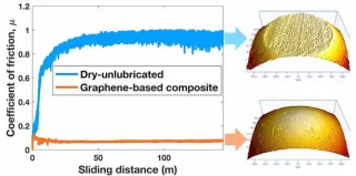
SOLID LUBRICANTS FOR EXTREME CONDITIONS
Lubricants are essential for a range of advanced manufacturing machinery, however, liquid lubricants struggle to perform under extreme conditions. Researchers at Purdue University have developed a new solid-state lubricant that is a viable option for extreme operating environments. The new liquid-free lubricant is a composite made from a slurry of graphene and zinc oxide nanoparticles bound together with polyvinylidene difluoride. Graphene has properties of extreme mechanical strength and ultralow friction while the zinc oxide enables durable binding of graphene to the contact surfaces. This new type of non-liquid lubricant has been shown to significantly reduce friction and wear under extreme conditions.
– Vilas Pol & Farshid Sadeghi, Purdue University
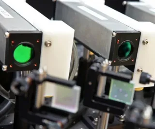
1,000-FOLD IMPROVEMENT ON THE RESOLUTION OF TIME-OF-FLIGHT MEASUREMENTS
Researchers at the Massachusetts Institute of Technology presented a new way of using time-of-flight optical measurements, the basis for Lidar technology, to significantly improve the resolution of distance measurements. The team combined methods from optical interferometry and from Lidar to get the best aspects of both. The result is an optical system that can measure objects two meters away with three micrometer resolution using optical components already available. The technique can be applied to autonomous vehicles as well as a whole host of manufacturing applications where distance is important but optical triangulation or other types of optical sensors are unsuitable.
– Achuta Kadambi & Ramesh Raskar, MIT
MAKING IMPROVED AND INEXPENSIVE ELECTRODES FOR SUPERCAPACITORS
Supercapacitors can store and deliver energy faster than batteries, but they tend to have lower charge capacity. A team of engineers at the University of Washington developed a supercapacitor electrode material with improved capabilities. Ultra thin sheets (10 – 100 atoms-thick) of WS2 or MoS2 are promising materials for boosting charge capacity, however they are limited by mechanical stability. To provide mechanical support, the team embedded the thin sheets into a carbon aerogel (which can act as a crude electrode itself), resulting in 127% higher capacitance than the aerogel alone. The team expects to reach higher capacitance with thinner WS2 or MoS2 sheets. This supercapacitor material was made using a refined method for making aerogels that is much faster than established methods, making it especially attractive for advanced applications.
– Peter Pauzauskie, University of Washington
SCALABLE AND COST-EFFECTIVE MANUFACTURING OF THIN FILM DEVICES
Engineers at Rutgers University–New Brunswick and Oregon State University are developing a new method of processing nanomaterials that could lead to faster and cheaper manufacturing of flexible, thin film devices – from touch screens to window coatings. The “intense pulsed light sintering” method uses high-energy light over an area nearly 7,000 times larger than a laser to fuse nanomaterials in seconds. The sharp reduction in temperature needed for fusion makes it possible to use low-cost, temperature-sensitive plastic substrates like polyethylene terephthalate (PET) and polycarbonate in flexible devices, without damaging them.
– Michael Dexter & Rajiv Malhotra, Rutgers University – New Brunswick

A NEW, INEXPENSIVE WAY TO FABRICATE MICRONEEDLES
A Tufts research team has devised a method to make microneedles without cleanrooms, using readily available materials and equipment. The process creates molds using a laser cutting technique that allows for the fabrication of different-size microneedles. Using a carbon-dioxide laser, which is readily available in many facilities, microscopic molds are etched on sheets of commonly used acrylic, employing a “crossover lines laser ablation technique.” The molds are then used to create degradable microneedles using inexpensive polyvinyl alcohol polymer. This process is easy to scale up, and only requires a laser cutter to create the molds.
– Sameer Sonkusale, Tufts University
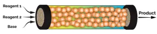
BOOSTING PHARMACEUTICAL MANUFACTURING EFFICIENCY WITH ‘GREEN’ CATALYSIS
Researchers at North Carolina State University have developed a green chemistry method that for the first time combines aspects of palladium-driven catalytic processes that are either (a) wasteful and fast or (b) minimally-wasteful and slow, to improve efficiency at a minimal cost of processing time. These palladium-driven catalytic reactions are used to connect carbons in small, organic molecules to create larger molecules for use in pharmaceuticals and synthesis of fine chemicals. The new continuous flow chemistry technique, called pseudo-homogeneous catalysis, relies on novel catalytic mircrospheres based on elastic silicone chemistry and created using microfluidics. One other advantage of the pseudo-homogeneous technique is that it makes use of nontoxic solvents, i.e., water and ethanol.
– Milad Abolhasani, North Carolina State University
BROMIDE-BASED ALUMINUM ELECTROPLATING FOR BETTER CORROSION PROTECTION
Parts made of steel, brass, copper, and other metals are commonly electroplated with aluminum to protect against corrosion. During deposition, aluminum ions can diffuse into the substrate metal to form a metallic interlayer that is critical to mitigate the corrosion of the structural components in a chloride environment. Electroplating at a relatively higher temperature promotes significant diffusion of surface aluminum to form the metallic interlayer with the substrate. Current electroplating solutions, made either from pure chloride melts or room temperature ionic liquids, are not carried out at sufficiently high temperatures to promote the formation of a robust diffused interlayer. Researchers at Idaho National Laboratory have developed bromide-based aluminum electroplating solutions that can be carried out at a relatively higher temperature (350°C), and so they are able to produce a much thicker, stronger, and uniform diffused metallic interlayer than just the surface aluminum coating usually formed from the other two electrolytes. The process, which can be used in the same setups as is currently used in commercial electroplating operations, also has less functional electrolyte loss and improved coating performance characteristics.
– Ryan Bills & Prabhat Tripathy, Idaho National Laboratory
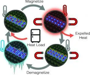
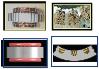
MAGNETIC POWERED REFRIGERATION
Vacuum tubes to chips. Incandescent bulbs to LEDs. Internal combustion engine to fuel cells. These are clear examples of the advantages of solid state devices over conventional counterparts. Researchers at GE Appliances and Oak Ridge National Laboratory have set out to add refrigeration to the list. At the core of this work are magentocaloric materials (MCM)—materials that respond thermally to magnetic field variations and promise to deliver 25% more efficient cooling systems than vapor-compression systems. They also may enable smaller, quieter, and more reliable systems. A major challenge in building a solid state refrigerator is forming magnetocaloric materials, such as La-Fe-Si, into the right shape to respond to magnetic fields and to transfer heat effectively. The team is developing novel methods to create structures of MCM.
– Ayyoub M. Momen, Oak Ridge National Laboratory
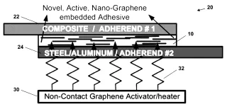
REVERSIBLE ADHESIVES FOR STRUCTURAL MULTI-MATERIAL JOINING
Adhesive joints have gained popularity due to their cost efficiency, light-weight designs, decreased stress concentrations, and ability to join dissimilar materials. However, adhesive-bonded joints commonly use thermoset adhesives, which are cured once and cannot be disassembled. A team at Michigan State University created a new adhesive that enables bonded joints with the ability to disassemble, repair and re-assemble. The new adhesive is composed of a thermoplastic material with embedded nano-scale or micro-scale particles, and works with any metal (aluminum, steel, magnesium, etc.), composite material or hybrid (multi-materials). Rapid, ‘targeted heating’ of the adhesive refreshes it, or allows it to be disassembled.
– Mahmoodul Haq, Michigan State University
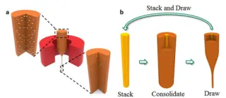
SCALABLE AND INEXPENSIVE PRODUCTION OF POLYMER-METAL NANOCOMPOSITE BY THERMAL DRAWING
Polymers embedded with metallic nanoparticles (polymer-metal nanocomposites) have unique physicochemical properties valuable for enabling electrically conductive polymer-based materials for transparent electrodes, electromagnetic interface shielding and electrostatic dissipation, electromagnetic wave absorbers for solar cells, and antimicrobial surfaces. Optimal performance of polymer-metal nanocomposites requires uniform dispersion of the metallic phase, however processes to fabricate such uniform nanophase dispersions are a long-standing challenge, and the techniques available today are often costly and difficult to scale. UCLA researchers have developed a polymer-metal nanocomposite fabrication method that achieves a uniform dispersion of the metallic nanoparticles based on traditional thermal drawing techniques. By using an iterative stack, consolidate, and draw process, non-uniform microparticles are transformed to evenly dispersed nanoparticles.
– Xiaochun Li, UCLA
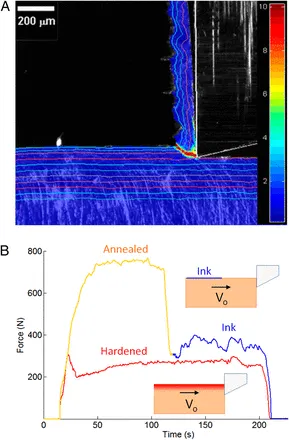
IMPROVED METAL MACHINABILITY
Annealed metals are notoriously difficult to cut, causing diminished tool-life, poor surface finish, and tool chatter. During cutting, thick chips build up in front of the cutting tool, increasing the cutting force and degrading cutting performance. Researchers at Purdue University have developed a method to suppress chip nucleation by coating the surface of the metals with a thin layer of marking ink (metal marking ink, containing colored pigments, propanol, and diacetone alcohol). The researchers believe the ink works by reducing the sinuous flow, the repeated folding of material, in front of the the cutting tool. This coating process could be used to cut structural metals such as stainless steel or aluminum and integrated with existing machining units through the addition of a suitably positioned nozzle or brush.
– Srinivasan Chandrasekar, Purdue University
FIGHTING AGAINST PRODUCT COUNTERFEITERS WITH AUTHENTICITY TAGS
InfraTrac uses chemical signatures to fight counterfeit products, a major scourge to U.S. manufacturing. In partnership with Penn State’s Center for Innovative Materials Processing, the technology was demonstrated in 3D printed metal parts. For example, in 3D printed titanium parts, “authenticity tags” are produced by slightly varying the feedstock composition just below the surface of the part. Here the tag can be easily detected with x-ray fluorescence spectroscopy, a fairly common laboratory tool with recent advances into handheld detection devices, without impacting the look or performance of the part. The location, depth, and composition of the authenticity tag can be varied from part to part such that only those who know exactly where to look and what to look for can find it, while those looking to fake the tag will be left guessing the specifics.
– Sharon Flank, InfraTrac
HIGHLY VERSATILE PRINTED ELECTRONICS USING NANOMATERIAL INKS
Printed electronics offer the promise of affordable, low volume, and bespoke electronics. Key to realizing this goal is printing highly versatile electronic components, such as transistors, at sufficient resolution. The Franklin Group has developed an aerosol jet printing process that enables the printing of nanomaterials with line widths as small as 10µm. The incorporation of nanomaterials facilitates the printing of transistors at higher resolutions and with improved performance and compatibility. An array of applications will benefit from this new combination of the additive manufacturing promise of aerosol jet printing and the unique properties of nanomaterials.
– Aaron Franklin, Duke University
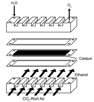
HIGH YIELD CONVERSION OF CARBON DIOXIDE TO ETHANOL
Converting carbon dioxide to a useful energy source, such as ethanol, would provide an essential renewable fuel source with a carbon negative process. Catalytic Innovations has developed novel catalysts and reactors that are able to improve conversion yields. The reactor uses an electrochemical process that leverages high pressure carbon dioxide, and is able to remove 10 gallons of carbon dioxide from the atmosphere for every liter of ethanol produced. This technology has additional applications in wastewater treatment, corrosion resistance, and a range of other areas.
– Staff Sheehan, Catalytic Innovations
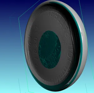
SILICON-BASED X-RAY OPTICS: THIN AND LIGHTWEIGHT
Reducing the size and weight of optics is essential for aerospace, defense, robotics, and a range of other areas. The use of single-crystal silicon, a first for X-ray optics, enables large collection areas with a thin, lightweight profile. Silicon also has a low response to thermal variation, and using single-crystalline silicon mitigates warping due to internal stresses during manufacturing. These properties ensure manufacturability and high quality optical performance.
– Will Zhang, NASA Goddard Space Flight Center
THERMALLY RESPONSIVE NANOPARTICLES FOR ENERGY SAVINGS
Vanadium oxide nanoparticles change how reflective or transparent they are to infrared light depending on temperature, making them attractive for applications in smart windows. Retrofitting windows in residential and commercial buildings with films laden with these nanoparticles has the potential to deliver energy savings of $12B/year in the United States alone. However, long term stability of the particles and scalable manufacturing processes are barriers to this technology. A team at Texas A&M recently developed a scalable manufacturing process to make vanadium oxide nanoparticles encased in a protective nanometer-sized silica sheath (which gives them long term stability), and to cast them on a film for use. The process itself is also environmentally friendly, designed to only use aqueous-based solutions over regulated organic solvent alternatives.
– Sarbajit Banerjee, Texas A&M University

ENABLING LOW-COST PRODUCTION OF NANOPOWDER THIN FILMS
The NanoSpraySM Combustion Processing technology can produce nanopowder and thin films at low cost. At the heart of the technology is an innovative liquid atomizer that can produce an aerosol of controlled size down to sub-micron range at fast flow rates without any atomizing gas. The ability to produce small-size droplets with narrow size distribution is of critical importance in the NanoSpraySM Combustion Processing technology, where precursor solutions are converted to a fine mist that is efficiently combusted in nanopowder and thin film deposition applications. This technology can be adapted to a wide variety of manufacturing environments, such as continuous web, wafer fabrication, and high volume individual parts.
– Andrew Hunt, nGimat
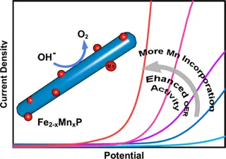
MANUFACTURING AFFORDABLE HYDROGEN FOR ALL
Splitting water to store energy in the form of hydrogen, a safe and clean gas, holds a strong appeal, but finding the right catalyst is key. Platinum or iridium-based materials, the current commercialized catalysts, have low overpotentials (i.e., high efficiencies) and long life, but are prohibitively expensive and there is simply not enough of these noble metals to go around. Prof. Stephanie Brock’s research group is zeroing in on base-metal phosphides combining first row elements such as manganese and iron, abundant and inexpensive materials. Her team is working to understand what makes these catalysts “tick” in order to design materials with improved performance and long-term catalytic stability. These materials are also of interest for next-generation catalytic removal of sulfur from fossil fuels, thereby reducing key contributors to respiratory illness and acid rain from combustion emissions.
– Stephanie Brock, Wayne State University
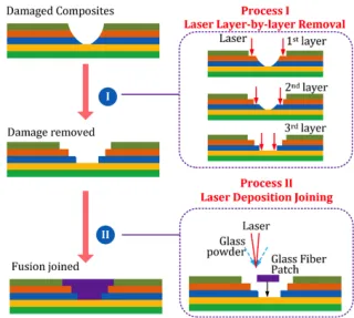
ENABLING FASTER AND STRONGER FIBERGLASS REPAIR
Repairing damaged composite parts is not as simple as welding two metal parts. Currently, repaired composite parts are epoxied together, which takes a long time and has low joint strength. Prof. Hongtao Ding is investigating new ways to repair composite parts used in industries ranging from automotive and aerospace to gas storage and wind energy. His approach is to add glass particles to the damaged area and then use a laser to melt the particles to encase the broken glass fibers together. His most recent results are promising and show that the melted glass particles bond strongly to the original fibers.
– Hongtao Ding, University of Iowa
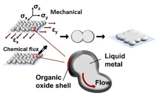
HEAT-FREE SOLDERING
Supercooled metal inks developed by SAFI-Tech enable soldering without needing to heat. The technology consists of water-balloon-like micro- and nanoparticles of liquid metal solders in a metastable supercooled state. These particles can be mechanically broken or chemically triggered to release the liquid metal, which then rapidly solidifies. The technology enables electronics manufacturers to speed up production and to solve manufacturing issues caused by high temperature processes, such as component degradation and mismatched coefficients of thermal expansion. This same technology has additional applicability in multi-material additive manufacturing, metal casting, and metal repair, where materials processing compatibility could be improved by lowering processing temperatures.
– Ian Tevis, SAFI-Tech
ADVANCED SILICON NANOTEXTURES IMPROVE PHOTOVOLTAICS, BIOSENSORS, & BATTERIES
Realizing the immense promise of silicon nanowires relies on the ability to control the arrangement and structure of the wires. Advanced Silicon Group has developed technology to create organized silicon nanowire arrays using metal-enhanced etching to texturize silicon. When modifying photovoltaic cells with these silicon nanotextures, solar energy capture can be enhanced by up to 1.5% (absolute). Unique capabilities of this technology include the ability to control the height, diameter, and density of the nanowires, reproducible uniformity over large surfaces, and a large-scale, low-cost industrial process. The technology also has emerging applications in biosensors, Li-ion batteries, and other fields.
– Bill Rever & Marcie Black, Advanced Silicon Group
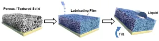
BIOINSPIRED SUPER SLIPPERY SURFACES
Slippery Liquid-Infused Porous Surfaces (SLIPS) consists of nano/microstructured substrates infused with a lubricating fluid, where the lubricant is locked in place by the substrate and forms a stable, defect-free, and inert “slippery” interface. This surface outperforms its natural counterparts and state-of-the-art synthetic surfaces in its capability to repel various simple and complex liquids (water, hydrocarbons, crude oil, and blood); maintain low contact angle hysteresis; rapidly restore liquid-repellency after physical damage; resist ice adhesion; and function at high pressures. Inspired by the insect-trapping Nepenthes pitcher plant, SLIPS will find important applications in fluid handling and transportation, optical sensing, medicine, and as anti-icing, self-cleaning and anti-fouling surfaces operating in extreme environments.
– Tak-Sing Wong, Penn State University
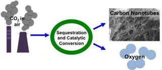
CONTROLLED CARBON NANOTUBE PRODUCTION IN LARGE QUANTITIES
SkyNano uses a process that converts carbon dioxide to carbon nanotubes. Carbon nanotubes exhibit remarkable properties including impressive mechanical strength, thermal conductivity, and electrical current capacity. The carbon nanotubes with the greatest potential are small diameter single-walled carbon nanotubes, which are difficult to produce in large quantity. SkyNano’s method uses an anode and a cathode to electrochemically reduce carbon dioxide into carbon and oxygen, but their breakthrough is in the combination of an inert anode and a catalyst coated cathode, which can produce carbon nanotubes with very small diameters reliably and inexpensively.
– Anna Douglas, Vanderbilt University & SkyNano Technologies
SCALABLE, SINGLE STEP FABRICATION OF 2D SEMICONDUCTORS ON CMOS
In order to be adopted, graphene and other 2D semiconductor materials need to be integrated with current methods of making integrated circuits, such as CMOS. This new method of fabricating 2D semiconductors uses standard microfabrication methods to grow self-contacted and self-aligned devices on CMOS chips in a single step. Parameters such as the type of metal used for the contact, temperature, time, pressure, and precursor quantity, provide means to tailor the growth. This technology has the potential to provide a scalable, front-end compatible, chemical vapor deposition (CVD) process to produce complex, conformal, self-contacted 2D materials-based devices. Specific applications for this technology include CMOS 2D materials-based devices, direct on-chip integration of sensors (optical, chemical, etc.), and flexible electronics.
– Eric Stinaff, Ohio University
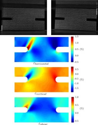
HIGH PERFORMANCE TOOLS FOR MEASURING STRAIN FIELDS IN DEFORMING COMPONENTS
Direct Strain Imaging™ (DSI) is an improved visual strain measurement technology using single or multiple cameras to track minute movements of dots applied to a component. It is now embodied in a system with precision, sensitivity and real-time data processing throughput that, in addition to standard tests, enables previously difficult tests such as measuring strain tensor component fields in rapidly moving components. Because of these features, as well as its ability to measure strain in components with complex shapes, the system is uniquely suited for post processing inspection and qualification of additively and traditionally manufactured components. This technology was licensed by the U.S. Naval Research Laboratory to Point Semantics for non-destructive evaluation in manufacturing and other disciplines.
– Brad Pantuck, Point Semantics Corporation
ADDITIVE MANUFACTURING FOR COMPLEX ALLOYS AND MICROSTRUCTURES
This new additive manufacturing method combines extrusion-based 3D-printing and sintering heat-treatments to create magnetic shape-memory alloy foams, wires, and micro-lattices. Shape memory alloys are useful because of their unique combination of low density, stiffness, high surface area, biocompatibility, compressive strength, and ductility. This novel manufacturing method doesn’t use lasers, e-beam, or powder beds, and the solvents allow for fast drying. These attributes open the potential for a manufacturing method that is fast, economical, and enables fine control over features and microstructures. This method has applications for actuators, energy harvesting, sensors, stents, bone implants, and more.
– Shannon Taylor, Ramille Shah & David Dunand, Northwestern University
HIGH-STRENGTH CONDUCTORS ENABLED BY COVETIC MATERIALS
Covetic materials are metals with about 4% of carbon nanostructures added in a way that leaves them much more thermally and electrically conductive than the metal alone. The carbon also enhances the metals’ oxidation and corrosion resistance and yield strength. Being able to enhance the electrical conductivity of even the best conductors, such as silver and copper, will have tremendous repercussions across the economy by conserving energy. Aluminum, the metal of choice in transmission and distribution cables, is thought capable of up to 40% higher conductivity when modified this way, according to the Department of Energy.
– Lourdes G. Salamanca-Riba, University of Maryland at College Park
BIOFABRICATING LEATHER
The young company Modern Meadow is working to scale up production of leather made by yeast cells engineered to make a collagen protein. The collagen self-assembles into fibers that Modern Meadow processes into sheets of “raw leather.” Leather manufactured this way uses less resources than leather made by livestock, it is more uniform and consistent, and it can span larger areas than that of the skin of a single animal. Biofabrication is an emerging method of growing materials by leveraging processes of organisms engineered for the task; akin to agriculture but taken to a whole new level. Manufacturers are working on addressing scale-up challenges to move biofabrication from the lab to the factory.
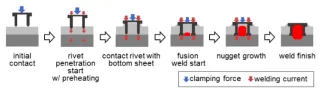
JOINING DISSIMILAR MATERIALS
Rivet Weld Technology opens up the use of lighter weight materials (e.g., aluminum) for key structures not previously considered due to the concerns with joining dissimilar materials. The rivet weld system is a hybrid joining process that combines the advantages of self-pierce riveting with resistance spot welding in a one-step process of joining dissimilar materials such as high strength steels to aluminum. This innovative technology addresses the limitations of existing methods of spot welding, self-piercing riveting, and adhesive bonding as a reliable and robust solution for dissimilar material joining. This new method of joining will have an impact on many manufacturing sectors, including automotive body in white assembly operations.
– Dan Radomski, Optimal Process Technologies
POTASSIUM BATTERIES
Lithium is categorized as a “critical material” by the Department of Energy and the Department of Defense leading researchers to investigate alternatives to lithium-ion batteries using potassium, which is chemically similar to lithium. For now, potassium batteries hold less energy than a battery made with the same amount of lithium, but potassium is far more abundant and cheaper. Adoption of potassium batteries requires the development of the right combination of cathode, anode, and electrolyte. A team of scientists and engineers from Purdue University, Oak Ridge National Laboratory, and National Cheng Kung University in Taiwan recently published a series of articles showing their progress towards finding the right anode material for potassium batteries.
– Vilas Pol, Purdue University

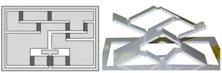
MULTI-COMPONENT, MULTI-MATERIAL, MULTI-PROCESS TOPOLOGY OPTIMIZATION (M3TO)
Traditionally, the choice of manufacturing method and part geometry were largely determined through a mix of experience, intuition, and availability. Structural topology optimization (TO) facilitates innovative designs by modeling arbitrary shapes to find those that that still meet the task while optimizing a certain parameter (e.g., mass). But existing TO methods fall short when it comes to designs that can be divided into parts made of different materials. Multi-component, multi-material, multi-process structural topology optimization (M3TO) is a one-of-a-kind method that simultaneously optimizes overall structural topology, part boundaries, and material-process selection in a single loop. Through the optimization results of what-if cases, the designer can also be informed of optimal ways to embed parts made of advanced materials and processes, such as metal 3D printing, within a structural assembly. This technology will help U.S. manufacturers merge design optimization, manufacturing, and materials considerations to produce high-performance, lightweight structures that are economical to manufacture.
– Kazuhiro Saitou, University of Michigan
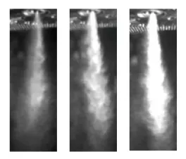
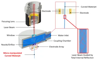
CURVED WATERJET-GUIDED LASER MATERIAL PROCESSING
Curved waterjet-guided material processing is a novel hybrid technique in the field of micro-manufacturing. It uses a laser beam confined within a waterjet, such that it combines the capabilities of laser and waterjet processing and adds a few advantages. For example, energy at the laser target is more uniform and the water serves as an optical guide and simplifies optical focus control allowing precision machining to a considerable depth. The electrode array facilitates the micro-manipulation of the jet’s trajectory and of its point of impingement on the workpiece for markedly enhanced processing accuracy and speed of response. The waterjet also cools the part and flushes material waste. The technology has applications in laser ablation, micro-cutting, surface micro-texturing and modification, and micro-incremental forming to mention a few.
– Kornel Ehmann, Northwestern University
ACHIEVING ULTRA-LOW FRICTION WITHOUT OIL ADDITIVES
A new surface treatment on metal surfaces allows for improved machine performance. The treatment changes how oil molecules bond with the metal, allowing for less oil to be used and eliminating the need for special additives without diminishing performance. Reducing friction on metal machinery using this new method can help manufacturers save energy and reduce fuel and oil consumption.
– Michael Varenberg, Georgia Institute of Technology
ENERGY EFFICIENT MANUFACTURING OF SHEET METAL
Producing sheet metal in a more efficient way can help reduce energy costs and the size of factory floors. A new process in development at Purdue University directly shaves sheet metal off a block in one go, as opposed to rolling it out repeatedly. Although the process won’t replace production of large sheets, it can help factories quickly and affordably produce smaller sections of sheet metals. Furthermore, the process works on less ductile metals that would otherwise crack with traditional processes.
– Srinivasan Chandrasekar, Purdue University
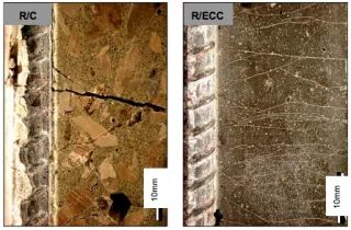
ENGINEERED CEMENTITIOUS COMPOSITES (ECC)
Engineered Cementitious Composites (ECC) is a new type of concrete designed to be damage tolerant and to continue carrying increasing loads even after cracks appear. The tight crack width of ECC also makes it much more durable than normal concrete or fiber reinforced concrete, leading to dramatic increase in service life. Sometimes referred to as bendable concrete or self-healing concrete, ECC offers a new window of opportunity to pre-fabricated construction, additive manufacturing of cement-based products, and durable civil infrastructure. ECC could help address challenges of the aging U.S. infrastructure.
– Victor Li, University of Michigan
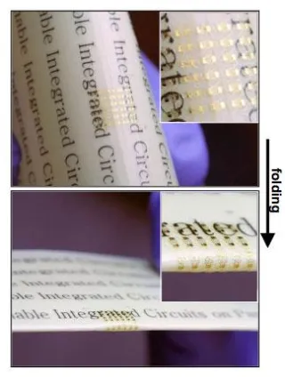
BIO-INTEGRATED STRETCHABLE ELECTRONICS
Researchers at Northwestern University are exploring classes of materials and assembly approaches that enable bio-integrated electronic devices with features that would be impossible to achieve using traditional, wafer-based technologies. These new stretchable electronics have exceptional area coverage, mechanical properties, or geometrical forms, enabling their integration directly onto biological tissue. This technology has applications in high-resolution mapping of electrophysiology in the heart and brain, battery-free blood oximetry, and bio-inspired photonics.
– John Rogers, Northwestern University
PRINTED GLASS OPTICS
Customized glass optics are needed in a range of areas, from lasers to optics to microfluidics. A new processes of creating these optics using 3D printing applies custom inks created from concentrated suspensions of glass particles. After 3D printing the transparent glass at room temperature, a thermal treatment is applied to increase density, and the part receives an optical quality polish. This new development could enhance the design and reduce the cost of manufacturing devices that incorporate optics, as well as accelerate microfluidics research.
[This work performed under the auspices of the U.S. Department of Energy by Lawrence Livermore National Laboratory under Contract DE-AC52-07NA27344 within the LDRD program. LLNL-ABS-738518]
– Rebecca Dylla-Spears, Lawrence Livermore National Laboratory

LAMINA EMERGENT MECHANISMS (LEMS)
Lamina emergent mechanisms (LEMs) are parts fabricated from a planar material (a lamina) that have motion that emerges out of the fabrication plane. They achieve their motion from the deflection of monolithic flexible members (rather than hinges), enabling simple manufacturing of parts that can obtain complex shapes and/or motions. The ability to fabricate them from planar layers of material makes it possible to manufacture LEMs using traditional planar processes, such as sheet metal or wafer fabrication. Applications range from MEMS devices for biological manipulation to novel low-cost consumer products.
– Larry Howell, Brigham Young University
DIODE-BASED ADDITIVE MANUFACTURING
In Diode-based Additive Manufacturing, the laser light is sourced by a set of four diode laser arrays and a pulsed laser. It passes through an optical valve, which patterns an image of a two-dimensional “slice” of the desired 3D part. The laser then flash prints an entire layer of metal powder at a time, instead of scanning with a laser as with traditional selective laser melting systems. The result is that large metal objects could be printed in a fraction of the time needed for metal 3D printers on the market today, expanding possibilities for industries requiring larger metal parts, such as aerospace and automotive.
[Text from article by Jeremy Thomas]
– Christopher M. Spadaccini, Lawrence Livermore National Laboratory
DUAL PHASE AND SOFT MAGNETICS IN ELECTRIC MACHINES
Magnets are a critical component of motors and alternators, driving their power density, form factor, and efficiency. New dual phase magnetic material and soft magnetics are being developed that can enhance and direct the magnetic field, improving these key performance metrics. These advances include novel chemical compositions, material topologies, and manufacturing methods of magnetic materials. Overall, these innovations have applications that can help create more efficient and effective manufacturing equipment, lower-weight electric vehicles, more energy efficiency electricity transformation, and more.
[This work was supported by the Department of Energy under agreement number DE-EE0007755.]
– Frank Johnson, GE Global Research
VAPORIZING FOIL ACTUATORS (VFA)
Forming and joining metals is challenging when joining dissimilar materials, forming complex shapes at low volumes, and shearing complex shapes. Vaporized Foil Actuation has the opportunity to overcome these challenges. This technology uses a very high energy deposition rate in a conductor to sublimate it before it has time to melt – vaporizing it directly into a gas. The result is a high-pressure pulse that, when physically constrained, can be harnessed as a tool to drive workpieces for forming or to develop high speeds for impact welding. Tools used with this technology technology are small, light, agile, and adaptable with little retooling for a wide variety of small-scale, impulse-based metalworking applications including impact welding, forming, embossing, shearing, and powder compaction.
– Glenn Daehn, The Ohio State University
ROLL-TO-ROLL ELECTRONICS USING PULSED THERMAL PROCESSING
Current methods of producing functional circuitry can be time consuming, require high temperatures, and reduce the ability to have design flexibility. Oak Ridge National Laboratory is developing roll-to-roll manufacturing techniques for thin film electronics utilizing unique Pulse Thermal Processing technologies coupled with non-vacuum low temperature deposition techniques. Successfully developing this technology for nanoparticle-based inks and pastes will allow for large-scale production of circuitry at reduced cost and energy requirements. Initial applications include processing thin film electronics on low-cost, flexible substrates such as polymers and paper, and may expand to include embedded circuitry in additive manufacturing components.
– Claus Daniel, Oak Ridge National Laboratory

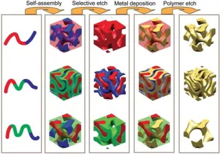
SELF-ASSEMBLY OF FUNCTIONAL MATERIALS
Self-assembly of Functional Materials merges the nanomanufacturing method of block copolymer self-assembly with the utility and functionality of a wide range of materials, from metals to ceramics to semiconductors. This manufacturing method enables the creation of otherwise difficult or impossible to fabricate structures by using self-assembly methods to form templates from which the geometry of functional materials can be shaped. This enables new classes of functional materials, with potential applications in fuel cells, solar cells, batteries, membranes, optics, life science research, and others.
– Ulrich Wiesner, Cornell University
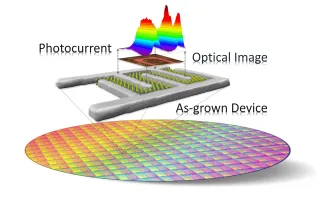
ATOMICALLY-THIN INTEGRATED CIRCUITRY
2D (atomically-thin) materials such as graphene and MoS2 hold enormous promise for creating the next generation of electronics and sensors using atomically-thin integrated circuitry. Inspired by the analogy of these 2D materials to paper, novel manufacturing methods have been developed to obtain desired shapes and material integration. Delamination techniques allow the materials to be moved, patterned, and stacked, to form complex 3D interconnects. This technique opens the ability to improve the performance of existing electronics and create structures with novel electromagnetic behavior, with applications in solar panels and nano-sensors.
– Jiwoong Park, University of Chicago
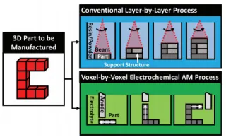
ELECTROCHEMICAL ADDITIVE MANUFACTURING (ECAM)
Electrochemical Additive Manufacturing (ECAM) is a novel manufacturing method that is capable of producing complex shaped functional metal parts layer-by-layer directly from computer generated 3D CAD models. ECAM process has the potential to overcome several of the limitations of traditional AM techniques, such as material choice, anisotropy, porosity, strength, scalability, support structure, and internal stresses. ECAM uses electrochemical deposition, a nonthermal process that uses electrical current to deposit cations or anions onto a surface. The processes has considerably lower residual stresses, and the addition of material is atom by atom resulting in excellent microstructural properties which can be controlled in process. ECAM is capable of depositing conductive materials including metals, metal alloys, conducting polymers, and even some semiconductors.
– Murali Sundaram, University of Cincinnati (This work is funded by the National Science Foundation.)
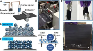
SOLVENT-FREE MANUFACTURING OF ELECTRODES FOR LITHIUM-ION BATTERIES
Lithium ion battery electrodes can be manufactured using a new, completely dry powder painting process. Unlike slurry-cast electrode manufacturing, solvent is not needed. Instead, the electrode goes through a hot rolling process, significantly decreasing thermal activation time. Removing the solvent and drying process allows large-scale Li-ion battery production to be more economically viable in markets such as automotive energy storage systems.
– Heng Pan, Missouri University of Science & Technology
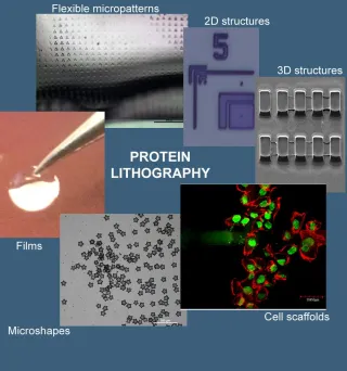
PROTEIN LITHOGRAPHY
Protein Lithography extends traditional lithography used in semiconductor manufacturing to the patterning of protein-based materials. This enables the creation of biopolymers with precise geometries as small as a few microns. Using proteins derived from silk, this fabrication technique opens up applications inaccessible to synthetic polymers. The use of benign solvents further enables applications that require biocompatibility. Protein lithography may prove beneficial in self-assembly, biosensing, therapeutic delivery and optical applications.
– Vamsi Yadavalli, Virginia Commonwealth University
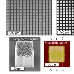
FLEXOGRAPHY USING NANOPOROUS STAMPS
Higher-resolution flexography is essential to manufacturing low-cost, large-area printed electronics and current production methods are limited in size due to contact-mediated liquid instabilities. Flexography Using Nanoporous Stamps can achieve continuous of micron-scale features with uniform nanoscale thickness at ~m/s speeds. This represents a combination of resolution and throughput that far surpasses current industrial printing technologies. The nanoporous stamp technology could be used to build machines for printing electronics in new formats, such as for large displays, smart packaging, and ubiquitous wireless sensors.
– John Hart, MIT
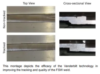
ENHANCED TRACKING AND CONTROL FOR FRICTION STIR WELDING
Friction Stir Welding is a solid-state joining process in which two metal pieces are joined together via mechanical intermixing; it is often used in building cars, trains, robots, ships, and more. Through the Tool Tracking for Friction Stir Welding is a technique to keep a weld tool on track by utilizing only force sensors on the friction stir welding tool. It’s beneficial for manufacturing since it can do corrections in real time, is cost-effective since no other sensors are required, and increases the robustness of the Friction Stir Welding process.
– Alvin Strauss and George Cook, Vanderbilt University
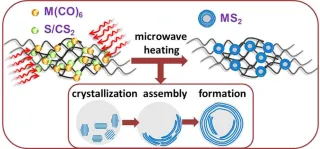
MICROWAVE-INITIATED ULTRAFAST NANOMANUFACTURING
Current processes for manufacturing metal oxides or sulfides can be complicated. A new technique using microwave-assisted heating, is an ultrafast and more energy-efficient method of manufacturing these nanomaterials. Microwave-initiated Ultrafast Nanomanufacturing can make it much quicker and lower cost to mass-produce these nanomaterials that can be used in lubricants, solar cells, lithium-ion batteries, and high performance protective composites.
– Xinyu Zhang, Auburn University
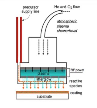
MANUFACTURING FUNCTIONAL AND TRANSPARENT COATINGS
Atmospheric pressure plasma discharge is used to fragment and polymerize small molecules as a method of Manufacturing Functional and Transparent Coatings. The manufacturing process can grow a wide range of materials, including silica, metal oxides, nitrides, and polymer coatings, onto both organic and inorganic substrates. There are obvious benefits for scalability by using a naturally abundant gas like compressed air to facilitate a coating process. Additionally, there is a significant reduction in chemical waste during the manufacturing process.
– Reinhold Dauskardt, Stanford University
NANOROBOTICS PLATFORM FOR NANOMANUFACTURING
A new Nanorobotics Platform for Nanomanufacturing combines controlled movement of nanorobots with unique light focusing or blocking abilities for direct surface writing and provides researchers with considerable freedom for creating diverse features with different shapes and sizes. This versatile production method could lead to a new ‘on-the-fly’ nanomanufacturing platform and create new opportunities for surface science and the production of nanodevices which could be used in a variety of fields including computers, energy, chemicals, and more.
– Joe Wang, University of California – San Diego
OPTICAL-TWEEZERS-BASED ADDITIVE FABRICATION
Optical-tweezers-based Additive Fabrication is being explored to enable the rapid additive fabrication of 3D microarchitectures and nanostructures that consist of tiny particles of various shapes (e.g., spheres, wires, and flecks) and materials (e.g., metals, ceramics, and polymers), which are simultaneously and individually moved, positioned, and joined together using a multiplicity of coordinated optical traps (i.e., focused laser light that induces stable trapping forces on tiny objects). The ability to manipulate tiny particles in this way can enable the creation of advanced microarchitectured materials which could be useful in many fields including civil engineering, electrical engineering, computing, and more.
– Jonathan Hopkins, UCLA

BIOPRINTED TISSUES
Bioprinted Tissues can offer a more precise platform for modeling disease and screening new drugs. 3D printers use a special hydrogel ink to print channels for tissue vasculature, then cells are injected to line the walls. This technology is a stepping stone toward realizing the dream of 3D printed organs.
– Jennifer Lewis, Harvard University
COLD SINTERING PROCESS (CSP)
LorCold Sintering Process (CSP) opens a window on the ability to combine incompatible materials, such as ceramics and plastics, into new, useful compound materials, and to lower the energy cost of many types of manufacturing. This process allows stronger materials to be created at lower temperatures which reduces the cost of production. The end result is better materials for use in architecture, biomedical implants, and many types of electronic components.
– Clive Randall, Penn State University
2D CRYSTAL CONSORTIUM – MATERIALS INNOVATION PLATFORM (2DCC-MIP)
The 2D Crystal Consortium – Materials Innovation Platform (2DCC-MIP) is focused on the development of two dimensional (2D) chalcogenides for applications in next generation electronics beyond silicon for digital circuits and flexible electronics. These materials include films that are only a few atoms thick, films that only conduct on the 2D surface, and multilayers of films whose properties are dominated by 2D interfaces. These new materials can be used to improve computing, displays, and communication.
– Joan Redwing, Penn State University (National Science Foundation cooperative agreement DMR-1539916)
MForesight’s work was supported by the National Science Foundation from 2015 to 2020 under Grant No. 1552534 to the University of Michigan (Dr. Sridhar Kota).
Please note that any opinions, findings, and conclusions or recommendations expressed on this website do not necessarily reflect the views of the National Science Foundation or the University of Michigan.
